
Research on LED Light Source System for PCB ThICk and Dense Circuit Detection
The improvement of process inspection capability of PCB board is directly related to the actual capability and long-term development of electronic products in domestic and foreign electronic industries With the development of PCB technology, PCB s has shown three major development trends: thinner lines, SMAller and higher line spacing, and more obvious height difference. This trend has been more obviously promoted and reflected in the past five years;, The instrument development PCB board industry is very backward at home and abroad The main reason is limited by the development of light source technology If the light source can not effectively realize the lighting and information selection of the object of interest, back-end measurement technology, including the application of image processing computing technology, precision electromechanical technology positioning, etc It is greatly restricted In response, many scholars at home and abroad have conducted extensive and in-depth experimental research and theoretical analysis Due to the improvement of the light source lighting system itself, in addition to improving the image clarity and contrast, it is more important to ensure the authenticity of the information selected from the image Many scholars' research is based on the direct improvement of image quality The direct consequence of adopting SIMilar research methods will increase the difficulty of precision control, which is very unfavorable to industrialization and scientific detection 2. In 2006, Li studied the key technologies of machine vision light source and developed a color ring layered LED light source applied to electronic component placement system, which directly improved the light source system to obtain better images, and then improved the accuracy The PCB board is taken as the direct research object, and the comparative research method combined with the real object is adopted. The light source illumination and image, in addition to effectively obtaining high image quality, the test characteristics of the actual object can also echo the optical design process of the light source Therefore, effective control of measurement accuracy can always be maintained in the process of light source design The lighting effect of the 50 ° LED ring light source developed in this paper is different from the current ordinary dark field low angle light source, and can clearly and truly reflect the PCB board However, it is worth noting that since the LED light source is used to detect the PCB with thick and close circuit s, it is important for PCB related test instruments If it is not tested, blindly applying it to other test instruments may result in poor lighting effect or system error
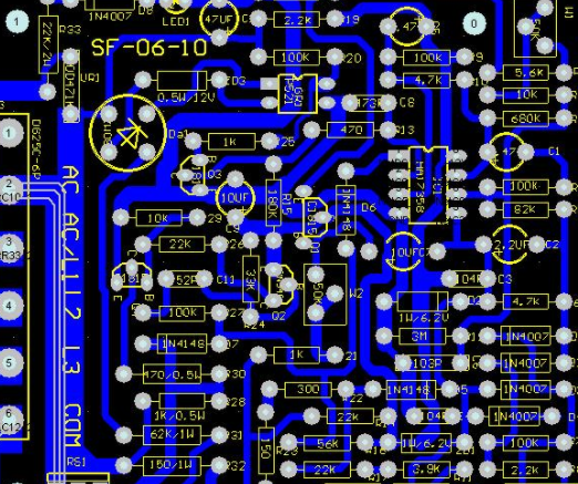
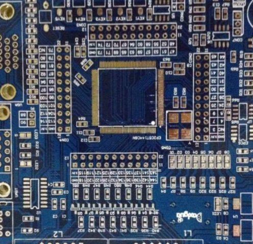
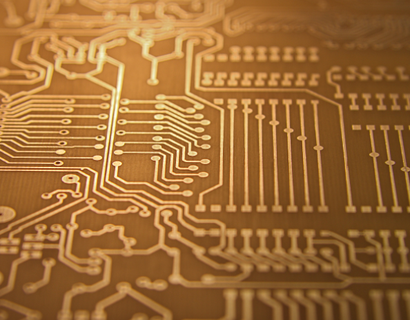
PCB board

1. Basic theory
1.1 Difficulties in the design of thick and dense plate light sources
In the development of the PCB industry, there are currently three major trends: thinner lines, smaller line spacing, higher density, and more obvious height difference The thick dense plate used in this paper is the concentrated embodiment of this trend As shown in Figure 1 (a), it is applied to PCB boards with larger line spacing and smaller thickness Figure 1(b) is the light path of a common light source applied to a PCB with a small line spacing and a large thickness. When the common light source is applied to PCB with large line spacing and small thickness, the substrate can illuminate the bottom and top of the line with good contrast It well reflects PCB board When applied to thick and dense plates, ordinary light sources are easily blocked by thick and dense lines due to the small light angle Therefore, the lines and the substrate have no good contrast and brightness that can be distinguished by the naked eye This makes further measurement based on image processing very difficult It can be seen that the problems caused by the development of thick and dense plates cannot be solved by ordinary light sources
1.2 Principle of adaptive ring light source based on fixed-angle design
From the previous analysis, it can be seen that in order to solve the problem of light source illumination of dense thick plates, stability and accuracy can be improved at the same time According to the geometric and optical characteristics of thick plates, it is necessary to effectively solve the selection of the incident angle and parameter configuration of the annular light source suitable for the application object Therefore, a self - adjusting ring light source based on a fixed angle design is proposed It consists of a ring housing/circuit board/LED/diffusion board The inner and outer ring housings are used to secure the entire light source and internal components There are series and parallel lines on the Flexible circuit board to supply power for LED As a light EMItting device, LED is an approximate point light source The emitted light has good directivity and is easy to be illuminated into highlights Due to the power characteristics of CCD, the area forming highlight will affect the output of adjacent points, thus affecting the measurement accuracy Therefore, a diffuser is installed in front of the light source used in this article to uniform the brightness of the light
2. Experimental results and discussion
2.1 Pseudo image error caused by ordinary light source illumination
The image captured by the current common light source has obvious edge deviation from the real cross-sectional view. When magnified twice, the size of the object surface corresponding to one point is 1.61m The line width difference caused by the edge of the pseudo image is greater than 3 points This greatly reduces the system accuracy The cause of false image edge is that the illumination angle of ordinary light source is too small After most of the light is blocked by dense thick lines, the brightness and color of the substrate are very close to the lower line width In general line width test, this deviation is not included in the measurement results A systematic error occurs in the inherent direction of the measured value, that is, if the error cannot be eliminated, the measured data is not a reflection of the real circuit characteristics of the PCB However, this error cannot be eliminated by changing the definition and contrast of the image This situation can only be eliminated or reduced by changing the design of light source according to the characteristics of thick lines and dense lines of PCB
2.2 Influence of geometric features of thick and dense lines on light source design
The line height/line spacing ratio is close to 1/2. That is, the angle is 27 ° When thick and dense plate is used as the line inspection object, the light incidence angle of the required light source is much greater than the light angle provided by the ordinary light source To obtain a clear contrast image, the angle of the light source must be increased to an appropriate value, taking into account the optical characteristics of the substrate and the circuit
2.3 The fixed-angle adaptive ring light source designed in this paper
Based on the above conditions, this paper designs an annular light source specially designed for thick and dense PCBs In order to evaluate the actual effect of the light source, the light source and the lens are aligned to the PCB in the same area, and the lens magnification is adjusted to the same Using the common light source can only illuminate the line with the normal direction close to the horizontal 45 ° near the line width, such as the two horizontal bright lines in Figure 5 (a) Due to the strong blocking effect of thick and dense lines on the light, the brightness of the substrate is very low, close to the brightness of the lower line width, and the difference between meat and meat is almost indistinguishable Because the reflection of the line surface is close to the specular reflection, the light reaching the line surface cannot enter the light receiving cone of the lens, and the brightness within the line width is also very low The image cannot effectively record PCB board, the line width accuracy analyzed is very low, and there is a fixed systematic error in the line width The image with self - adjusting light source designed in this paper has good uniformity and clarity Due to careful consideration of the light source angle, the brightness of the substrate/circuit transition/circuit surface rises step by step, and the transition area between different features is small, which is conducive to improving the test accuracy and realizing the lighting and information selection of the circuit of interest Ideal source image for image processing
3. Conclusion
In order to solve the problem of the existing common light source for the inspection of thick and dense lines on PCB boards, this paper analyzes the illumination artifact error of common low angle light sources, and discusses the influence of geometric and optical characteristics of thick lines and dense lines on light source design, A special light source for PCB circuit detection based on fixed angle design is proposed and designed The experiment shows that the lighting effect of this light source is different from that of the ordinary dark field low angle ring light source, and it can better solve the problems existing in the thick layer and dense layer detection currently. The PCB board comes from the front end of the system The illumination of the object of interest and the selection of accurate information are realized High image uniformity and good substrate contrast/transition area/line width This is of great significance to back-end image processing and information selection It can be widely used in PCBdetection equipment represented by line width detector
然后
聯(lián)系
電話熱線
13410863085Q Q

微信

- 郵箱


