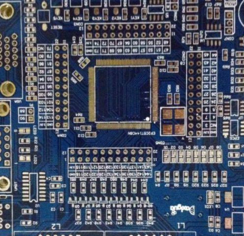

What spacing should be considered in PCB design
There are many aspects of PCB design that need to consider safe spacing In this case, it can be temporarily divided into two categories: one is power related safety distance, and the other is power independent safety distance
1. ElectrICal safety distance:
Conductor spacing
According to the processing capacity of leading PCB manufacturers, the spacing between conductors shall not be less than 4mil. Line distance is also the distance from line to line and from line to pad. From the perspective of production, if conditions permit, the larger the scale, the better. Generally, 10mil is more common.
PCB board

Pad hole diameter and pad width
According to the processing capacity of mainstream PCB manufacturers, if mechanical drilling is used, the hole diameter of the pad shall not be less than 0.2mm, and if laser drilling is used, it shall not be less than 4mil. The hole diameter tolerance varies from plate to plate. Generally, it can be controlLED within 0.05mm. The width of the pad shall not be less than 0.2mm.
Spacing between pads
According to the mainstream processing capacity PCB manufacturer, the spacing between pads should not be less than 0.2mm
Spacing between copper sheet and plate edge
The distance between the live copper sheet and the edge of PCB board shall not be less than 0.3mm. Set spacing rules on the design rule board outline page, as shown in the figure above.
If it is large area copper, it is usually required to have a shrinkage distance from the plate edge, which is generally set as 20mil. In the PCB design and manufacturing industry, generally speaking, in order to consider the finished circuit board machinery, or to avoid winding or power short circuit caused by the exposure of copper sheet on the board edge, engineers usually distribute copper blocks in a large area that shrinks 20 mils relative to the board edge, rather than extending to the board edge. There are many ways to treat this dented copper skin. For example, draw a keepout layer at the edge of the slab, and then set the distance between the copper and the keepout layer. A SIMple method is introduced here, which is to set different safety distances for copper cable laying objects. For example, the safety distance of the whole board is set as 10mil, and the copper cable laying is set as 20mil. It can achieve the effect of 20 mil edge shrinkage. At the same time, dead copper that may appear in the equipment is also removed.
2. Non electrical safety distance:
Character width height and spacing
During processing, you cannot make any changes to the text film unless the linewidth of characters with D code SMAller than 0.22mm (8.66mil) is increased to 0.22mm. That is, the character line width is L0.22mm (8.66mil). The width of the whole character is W1.0mm. The height of the whole character is H1.2mm. The character spacing is D0.2mm. When the text is smaller than the above standard processing, printing will become blurred.
Through hole to through hole spacing (hole edge to hole edge)
The through-hole spacing (edge to edge) is greater than 8mil.
Distance from screen to keyboard
Screen printing on a flat plate is not allowed. Because if the screen is covered by the mat, when the tin screen is not on the tin, the installation of components will be affected. Generally, 8 mil spacing is required to be reserved in the sheet mill. If the PCB board is solid in a limited area, the 4mil spacing is almost unacceptable. If the screen accidentally covers the pad during the design process, the Circuit board manufacturer will automatically remove the screen part left on the pad during the manufacturing process to ensure the tin on the pad.
Of course, it will be specifically analyzed in the specifIC design situation. Sometimes the mask is intentionally close to the pad, because when two pads are close, the mask in the middle can effectively prevent short circuit of solder joints during welding. This case is another matter.
3D height and leveling distance on mechanical structure
PCB components shall be installed horizontally, and the space height shall not conflict with other mechanical structures. This, in the design, the applicability of space structure between components and between PCB finished products and product shells shall be fully considered, and a safe space shall be reserved for each target object. Spacing is considered to ensure that they do not conflict spatially.
How to solve the problem of insufficient spacing?
The spacing is measured in the air (line of sight), which can be correctly arranged at the layout level to reduce the required spacing. Spacing can be significantly reduced by the use of insulating materials and, where possible, by bilateral assembly. The insulation layer can be a thin plate barrier between high-voltage nodes. Since high components are surface mounted, circuits that need to be spaced can be placed on both sides of the circuit board. Nodes with the same potential in the same high-voltage circuit usually need to be carefully separated from low-voltage circuits. A good method is to place a high-voltage circuit on the top of the circuit board and a low-voltage circuit on the bottom for control and monitoring. Low voltage circuits generally do not have the boundary surface (enclosure) creepage requirements required for high voltage circuits.
How to solve the problem of insufficient creepage distance?
We know that the creepage distance refers to the distance between power nodes on the insulating surface. In our discussion, this means the space between the surface or inner layer conductors of a PCB. However, the further expansion of the components will be limited by the product packaging volume. In this case, some other strategies are required to meet the required creepage distance and allow higher packaging density.
Standard for calculating conductor spacing under different voltage levels
Proper distance between PCB conductors is essential to avoid short circuits between conductors. Unfortunately, there is no single solution to this problem. There are various industrial and safety standards that specify different spacing requirements based on voltage, application, and other factors. The following are some precautions to help you determine the proper distance between PCB leads.
When products must pass safety facilities, each safety facility has a set of standards to meet specific insulation requirements. In this case, it is easy to find the required spacing. For example, in the United States, for most power or battery powered information technology equipment, the allowable PCB spacing should be determined according to Table 2K, 2L, 2M or 2N of UL IEC60950-1 version 2 standard. These tables specify the so-called safe distances and "creepage distances" for various insulation classes.
The level required depends on the position of the circuit. When considering the spacing and creepage requirements of a given design, consider the combination of pollution level and insulation type. The pollution level usually refers to the amount of dust, moisture and other particles on the surrounding air or the surface between high-pressure nodes. This standard specifies functional insulation, basic insulation, complementary insulation, double insulation and reinforced insulation. These definitions of insulation are quite complex. Creepage distance standards also vary with these insulation classes. The figure below shows the creepage distance required by IEC60950-1. Creepage distance required for different voltage levels. The data in the following table are used for basic insulation class. In case of double or reinforced insulation class, the data shall be doubled.
The above is the explanation given by the editor of pcb circuit board company.
If you want to know more about PCBA, you can go to our company's home page to learn about it.
In addition, our company also sells various circuit boards,
High Frequency Circuit Board and SMT chip are waiting for your presence again.
然后
聯(lián)系
電話熱線
13410863085Q Q

微信

- 郵箱


