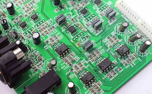
Do you know these scripts in PCB design and manufacturing industry!
Test Coupon: commonly known as impedance bar
It is used to measure whether the characteristic impedance of the PCB produced meets the design requirements with TDR. Generally, the impedance to be controlLED includes single ended line and differential pair. Therefore, the line width and line spacing (when there is differential pair) on the test coupler should be the same as the line to be controlled. The most important thing is the location of the grounding point during measurement.
Golden Finger
Gold finger is used to compress and contact the connection between the connector shrapnel for conductive interconnection. Gold was chosen because of its superior conductivity and oxidation resistance. Gold finger is the row of golden objects in the memory module or video card version of your computer.
Hard gold
Electroplating soft gold is to deposit nICkel and gold on the circuit board by electroplating, and its thickness control is flexible. Generally, it is used for making aluminum wire on COB (Chip On Board) or the contact surface of mobile phone keys. Most of the electroplating gold used for gold finger or other adapter cards or memory is hard gold, because it must be wear-resistant.
The difference between hard gold and soft gold is the composition of the last layer of gold plated. When gilding, you can choose to electroplating pure gold or alloy. Because the hardness of pure gold is relatively soft, it is also called "soft gold". Because "gold" can form a good alloy with "aluminum", COB will specially require the thickness of this layer of pure gold when making aluminum wire.
Through hole: Plating Through Hole (PTH for short)
The reason why copper foil layers cannot communicate with each other is that each layer of copper foil is paved with an insulating layer, so they need to rely on via for signal link, so they have the Chinese name of via.
The through-hole is also the SIMplest kind of hole, because it is relatively cheap to use a drill or a laser to directly drill the circuit board.
Blind hole: Blind Via Hole (BVH)
The outermost circuit of a PCB is connected to the adjacent inner layer with electroplated holes. Because the opposite side cannot be seen, it is called a "blind hole". In order to increase the space utilization of PCB circuit layers, the "blind hole" process CAMe into being.
The blind hole is located on the top layer and bottom layer of the circuit board, and has a certain depth. It is used to connect the surface layer circuit with the lower inner layer circuit. The depth of the hole generally has a specified ratio (aperture).
Buried Via Hole (BVH)
Buried hole refers to the connection between any circuit layers in a printed circuit board (PCB), but it is not conductive to the outer layer, that is, there is no conductive hole extending to the surface of the PCB.
Next, let's compare the advantages and disadvantages of different PCB surface treatment processes and applicable scenarios.
Advantages: low cost, smooth surface, good weldability (without oxidation).
Disadvantages: It is easy to be affected by acid and humidity, and cannot be kept for a long time. It needs to be used up within 2 hours after unpacking, because copper is easily oxidized when exposed to the air; It cannot be used for double-sided boards because the second side has been oxidized after the first reflow soldering. If there are test points, solder paste must be printed to prevent oxidation, otherwise it will not be able to contact the probe well in the future.
HASL, Hot Air Solder Levelling

Advantages: low price, good welding performance.
Disadvantages: It is not suitable for welding pins with thin gaps and too SMAll components, because the surface flatness of tin spraying plate is poor. Solder beads are easy to be produced in PCB processing, which is easy to cause short circuit to fine pitch components. When it is used in double-sided SMT process, because the second side has undergone a high temperature reflow soldering, it is very easy to produce tin beads or similar water droplets that are affected by gravity into dripping spherical tin spots due to the re melting of tin spraying, resulting in more uneven surface and thus affecting the welding problem.
Tin spraying process was once dominant in PCB surface treatment process. However, tin spraying process is an excellent process for larger components and wires with larger spacing. In PCB with high density, the flatness of tin spraying process will affect the subsequent assembly; Therefore, HDI boards generally do not use tin spraying process. With the progress of technology, the tin spraying process for QFP and BGA with smaller assembly spacing has appeared in the industry, but it is rarely used in practice.
OSP (Organic Soldering Preservative)
Advantages: It has all the advantages of bare copper plate welding. The expired (three months) plates can also be re surface treated, but usually only once.
Disadvantages: easily affected by acid and humidity. When it is used for the second reflow soldering, it needs to be completed within a certain time, and the effect of the second reflow soldering is usually poor. If the storage time exceeds three months, the surface must be re treated. Use up within 24 hours after unpacking. OSP is an insulating layer, so the test point must be printed with solder paste to remove the original OSP layer before contacting the pin point for electrical test.
The OSP process can be used on low technology PCB or high technology PCB, such as single side TV PCB and high-density chip packaging board. For BGA, there are also many OSP applications. If PCB has no functional requirements for surface connection or storage period limitation, OSP process will be the most ideal surface treatment process. However, OSP is not suitable for a small number of diverse products, nor for products with inaccurate demand estimates. If the company's PCB inventory often exceeds six months, it is really not recommended to use OSP surface treated boards.
ENIG, Electroless Nickel Immersion Gold
Advantages: It is not easy to oxidize, can be stored for a long time, and the surface is flat. It is suitable for welding thin gap pins and components with small solder joints. Preferred for PCB boards with keys. Repeated reflow soldering is not likely to reduce its solderability. It can be used as the base material for COB (Chip On Board) wiring.
Disadvantages: The cost is high, and the welding strength is poor. Because of the use of electroless nickel plating process, it is easy to have the problem of black disc. The nickel layer will be oxidized over time, and long-term reliability is a problem.
The gold deposition process is different from the OSP process. It is mainly used on boards with connection functional requirements on the surface and a long storage period, such as the key contact area, the edge connection area of the router shell, and the electrical contact area of the elastic connection of the chip processor. Because of the flatness of tin spraying process and the flux removal of OSP process.
ENIG, Electroless Nickel Immersion Gold
Silver deposition is cheaper than gold deposition. If PCB has connection functional requirements and needs to reduce costs, silver deposition is a good choice; In addition, the good flatness and contact of silver deposition make it more appropriate to choose the silver deposition process.
ENIG, Electroless Nickel Immersion Gold
It is often found that the partners are confused about the gold sinking and gold plating process. Let's compare the differences and applicable scenarios between the gold sinking process and gold plating process
The crystal structure formed by gold deposition is different from that formed by gold plating. The gold plated plate is easier to weld than the gold plated plate and will not cause poor welding;
Only the pad of the gold plate has nickel gold, and the signal transmission in the skin effect will not affect the signal in the copper layer;
The crystal structure of gold deposit is denser than that of gold plating, and it is not easy to oxidize;
Only the bonding pad of the gold plate has nickel gold, which will not produce gold wire and cause slight shortness;
Only the bonding pad of the gold plate has nickel gold, and the resistance welding on the circuit is more firmly combined with the copper layer;
The sunken gold shows golden yellow, which is more yellow and beautiful than the gilded gold;
Gold plating is softer than gold plating, so its abrasion resistance is not as good as gold plating. For gold finger board, the gold plating effect will be better.
PCB manufacturing, PCB design and PCBA processing manufacturers will explain the scripts of PCB design and manufacturing industry.
然后
聯(lián)系
電話熱線
13410863085Q Q

微信

- 郵箱


