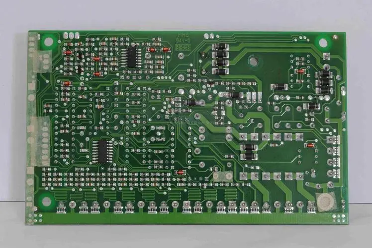

The wire of ultra precision six layer PCB is refined, and the through-hole is miniaturized, whICh improves the requirements for the control level of processing equipment and process of PCB processing plants, and also tests the overall management ability of precision six layer PCB factory and the personal ability of employees. The 6/6mil line width/line distance manufacturing capability is not too difficult within the current equipment, materials and process control level, and most PCB manufacturers can make it. However, it is a big leap from 6/6mil to 5/5mil, which makes many SMAll and medium-sized manufacturers sigh. It seems SIMple, but in fact, it requires that PCB manufacturers have strong technical research and development capabilities and financial strength. Subject to the performance parameters of the exposure machine, the processing ability of the etching line, and the control ability of the whole process, the strong overall strength of the Pcb factory is required to support the 5/5mil circuit and maintain a high yield. Similarly, the same is true for the fabrication of finished hole diameters of 0.3mm and below (holes of 0.3mm and below cannot be drilLED by machine, and are generally laser drilled)

The Importance of PCB as the Carrier of Electronics
As the carrier of all electronIC components, PCB reliability is very important. A small hair and a small dust may cause the whole PCB to be scrapped, or lead to potential failure hazards. How is the quality guaranteed? It is generally believed that quality should be produced, but it is not. If a PCB factory can adjust, control and prevent common quality problems from the perspective of effective quality control at the beginning of design, including PCB factory layout, determination of PCB process flow, selection of production equipment, manpower allocation, effective evaluation of raw materials, determination of management system, etc., and fully consider improving production efficiency, The future quality control ability and production capacity of this factory will have a good foundation and guarantee.
What should be prepared in advance before pcb board proofing
Generally, PCB board proofing is done for testing before experiments or mass production of PCB boards. PCB files have many forms. to meet different MARKet needs, PCB board manufacturers can open these different forms of files. So, what data should be prepared before pcb board proofing? Follow to learn!
Generally, it is necessary to provide pcb or GERBER documents to PCB manufacturers, and the documents provided should include some board making instructions, such as the number of board layers, required materials, pad process, ink color and other specific Production requirements. The details are as follows:
1. Materials: It is required to specify what materials are needed to produce PCB. Generally, FR4 is commonly used, and the main material is epoxy resin peeling fiber cloth board.
2. Board layer: after pcb board proofing, the number of layers has an impact on the price, so the number of layers should be noted.
3. Soldering resistance color: the normal color is green, and other colors shall be indicated.
4. Silk screen color: the color of the font and border of the silk screen on the PCB board, which is generally white by default.
5. Copper thickness: generally, the copper thickness is calculated scientifically according to the current of the circuit. Generally, the thicker the copper is, the better, but the cost will be higher, so it needs to be balanced reasonably
Whether the vias are covered with resistance welding: resistance welding is to insulate the vias, otherwise the vias will not be insulated.
6. Surface coating: before pcb board proofing, it shall be stated that the surface coating is tin spraying or gold plating.
7. Quantity: the quantity of pcb shall be clearly stated.
然后
聯(lián)系
電話熱線
13410863085Q Q

微信

- 郵箱


