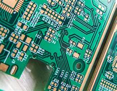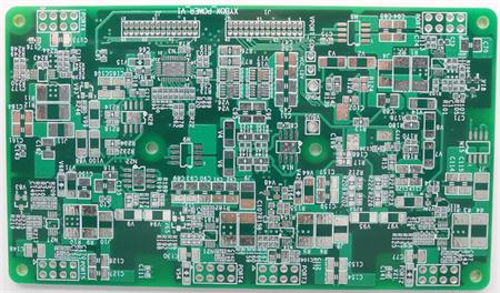

1. DiSMAntle the components on the single-sided printed PCB board: toothbrush method, screen method, needle method, tin suction devICe, pneumatic suction gun and other methods can be used. Table 1 provides a detaiLED comparison of these methods.

Most of the SIMple methods for disassembling electronIC components (including the foreign advanced pneumatic suction gun) are only suitable for single panel, but not good for double-sided PCB boards and multilayer PCB boards.
2. Dismantle the components on the double-sided PCB board: single side integral heating method, needle tube hollowing method and tin flow welder can be used. The single connected integral heating method requires special heating tools, which is inconvenient for general use. Needle tube hollowing method: First, cut off the pins of the components to be removed and remove the components. At this time, the cut pins of the components are left on the printed PCB board. Then, melt the tin on each pin with a soldering iron and take it out with tweezers until all pins are removed. Then, use a medical needle appropriate to the inner diameter of the bonding pad hole to empty it. Although there are several processes, this method has no impact on the printed PCB board, It is easy to obtain materials and operate, and it is extremely easy to realize. After years of practice, I think it is an ideal method.
3. Dismantle the components on the multi sided printed PCB board: if the above methods are used (except for tin flow welder), it is not difficult to disassemble, or it is easy to cause layer to layer connection failure. Generally, the pin welding method is used to cut the component from the root of the pin, leave its pin on the printed PCB board, and then weld the pin of the new component on the pin left on the printed PCB board. However, it is not easy to weld the multi leg manifold block. The tin flow welding machine (also called the secondary welding machine) can solve this problem, and is the most advanced tool for disassembling the integrated blocks on dual and multi-layer printed PCB boards. However, the cost is relatively high, requiring thousands of yuan of investment. The tin flow welder is actually a special small wave soldering machine. It uses a tin flow pump to draw fresh and unoxidized molten tin from the tin pot, and then gushes out through optional tin spouts of different specifications to form a local small wave peak, which acts on the bottom of the printed PCB board. The solder of the pins and solder holes of the disassembled components on the printed PCB board will melt immediately in 1 to 2 seconds. At this time, the component can be pulled out gently, Then use compressed air to blow through the welding hole of the element, insert a new element again, and then weld the finished product on the wave crest of the tin jet mouth.
Of course, in addition to the above, there are other methods (such as copper wire method, alcohol lamp method, etc.), but because of its non prominent characteristics, it is similar to the above methods, so I will not talk about it here.
In daily life, most of the household appliances we use are single panel. Although various simple methods have their own characteristics, it is recommended to use a tin suction device. For double and multiple panels, the simple method mentioned above can be used. It is economical and feasible, and it is better to use the tin flow welder.
然后
聯(lián)系
電話熱線
13410863085Q Q

微信

- 郵箱


